13651969369

當(dāng)前位置:首頁 > 產(chǎn)品中心 > 二維材料 > 二維材料溶液 > HfSe2 Solution


簡要描述:HfSe2 solution has been created by suspending HfSe2 sheets into isopropanol solution but if needed other solution types can be arranged.
 更新時(shí)間:2024-06-03產(chǎn)品型號: 廠商性質(zhì):生產(chǎn)廠家訪 問 量:1238
詳細(xì)介紹
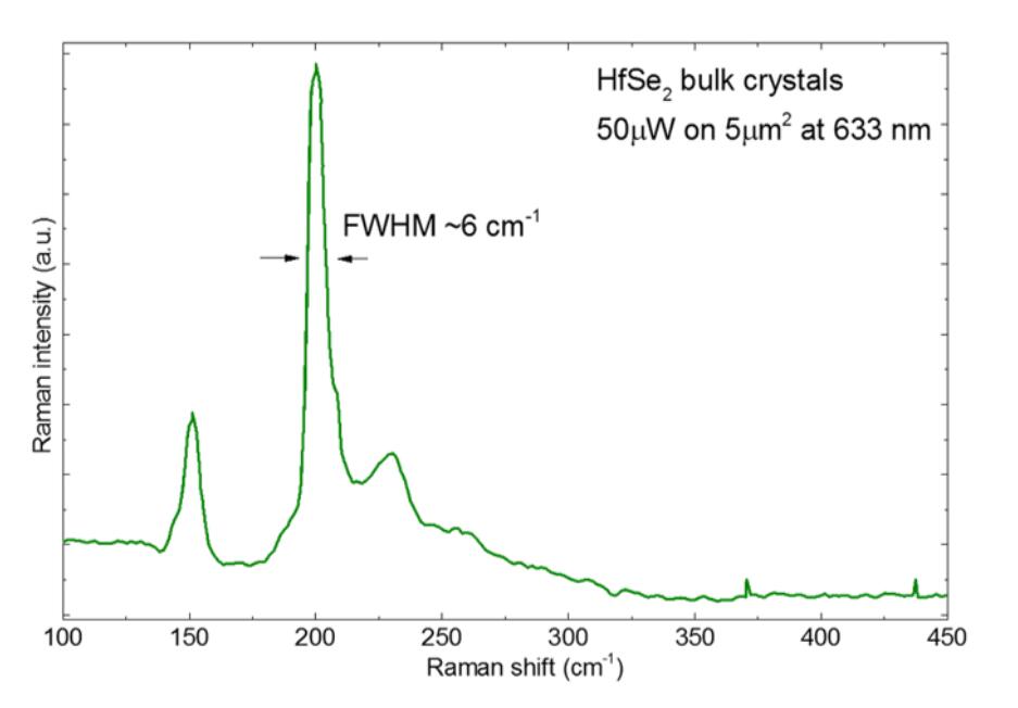
HfSe2 solution has been created by suspending HfSe2 sheets into isopropanol solution but if needed other solution types can be arranged. HfSe2 crystal precursors are developed at our facilities using state-of-art flux zone techniques. Each growth takes close to three months to provide you perfected crystals that does not contain any halides. Each crystal is highly crystalline, oriented in 0001 direction, and easy to exfoliate. Our R&D staff takes characterization dataset in each sample piece to ensure structural, optical, and electronic consistency. They have been optimized to achieve perfect industrial semiconductor grade materials with: 1) excellent stoichiometry, 2) large single domain size, 3) single phase materials without any mixed phases or amorphous content, 4) perfect layered crystal ideal for exfoliation purposes with impressive mosaic spread 0.08 degrees, 5) unmatched purity -semiconductor grade (6N), 99.9999%.
Solution type: By default 2Dsemiconductors USA will provide HfSe2 sheets suspended in isopropanol owing to good dispersion, stability, and high performance. However, if your research requires other solvents, please contact us for more details and schedule for the product delivery.
Solution concentration: To reduce shipping costs, easy customs agreement / border check-in processes, we ship supersaturated 2D solutions (~100 mg/L depending on the type of 2D layers). However, supersaturated solutions can be diluted to produce ~250-500mL of solution to deposit 2D layers onto desired substrates through simple and cost-effective spin-casting process.
Growth method matters> Flux zone or CVT growth method? Contamination of halides and point defects in layered crystals are well known cause for their reduced electronic mobility, reduced anisotropic response, poor e-h recombination, low-PL emission, and lower optical absorption. Flux zone technique is a halide free technique used for synthesizing truly semiconductor grade vdW crystals. This method distinguishes itself from chemical vapor transport (CVT) technique in the following regard: CVT is a quick (~2 weeks) growth method but exhibits poor crystalline quality and the defect concentration reaches to 1E11 to 1E12 cm-2 range. In contrast, flux method takes long (~3 months) growth time, but ensures slow crystallization for perfect atomic structuring, and impurity free crystal growth with defect concentration as low as 1E9 - 1E10 cm-2. During check out just state which type of growth process is preferred. Unless otherwise stated, 2Dsemiconductors ships Flux zone crystals as a default choice.


產(chǎn)品咨詢
 聯(lián)系人:陳谷一
 地址:江蘇省泰州市鳳凰西路168號
 郵箱:taizhou@sunano.com.cn
 電話:021-56830191
掃一掃以下二維碼了解更多信息

銷售微信咨詢

網(wǎng)站二維碼
 歡迎來到
歡迎來到